Making circuit boards with a CNC machine
Posted Oct. 29, 2018 by Dave GriffithsOne of the strategies we've been exploring at FoAM Kernow is using our hardware projects to research different ways of building things. For example our approach of design assuming collapse (& brexit) has resulted in much higher awareness of our supply chains, and through this - potential dependance on manufacturing in places with less environmental and health regulation.
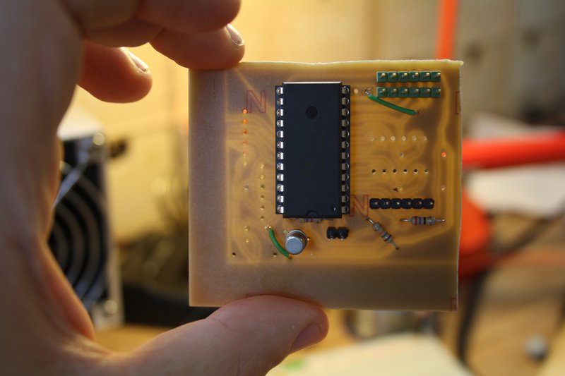
Printed circuit boards are problematic in this way. We tried out some experiments earlier in the year etching our own PCBs and soon after publishing our work on this blog, we were donated a small CNC machine to try out as an alternative method. We have now started using this for our prototypes and even short run production boards for projects like Viruscraft and Penelope.
Looking around online, it seems that people have quite varied success milling printed circuit boards, it can be very tricky - particularly using CNC machines that don't cost thousands, or are not specifically designed for the purpose. For us though, this has worked out well, and its becoming an essential part of our studio - particularly for very quick turn around or short runs of boards. One of the great things is that the same machine can drill exactly the right dimensions for all the components, and cut round whatever strange board outline you need - as well as milling out the copper so the circuit works. Sometimes you can even do all this without needing to change tools.
In terms of software, we are using the open source KiCad for designing the circuits and pcb2gcode to process the 'gerber' files KiCad produces and provide instructions for the CNC machine (a Roland iModela IM-01). Using this machine we can use a feed rate of 20-40 mm/minute which can mill a fairly complex PCB in around an hour.
Circuit design notes
There are considerations you need to keep in mind when designing for CNC milled boards. I'll get to end bit sizes in a moment, but the thing you need to consider is the track clearance needed for the end mill you are using - we started with a whopping 1mm clearance and track width, and with experimentation we've gradually reduced this down to 0.5 mm. This is pretty good for most purposes, but unfortunately it's not possible with this clearance to safely squeeze tracks between the 2.54 mm pins of normal through hole ICs - which is a bit of a pain if you're used to getting boards professionally manufactured at 0.2mm or so clearance.
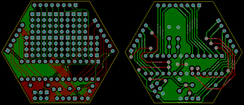
Above: an example of a design for professional manufacture on the left and a single sided CNC mill on the right for the same circuit. (The red tracks on the right indicate where jumpers wires need to go on the top side).
You also need to consider that milling away large areas of copper is quite wasteful (similar to etching, but more so) so you can either leave the unused areas unconnected, which may cause capacitance issues - or try and use properly grounded copper fill areas where possible, or alternatively you can use voronoi zones instead of tracks. The pcb2gcode program has an option to calculate these, and it essentially expands the tracks to the largest area possible so they all butt up against each other to use up all the copper, leaving no unconnected zones. This looks a bit strange, and it can make soldering a bit harder as your iron needs to heat larger areas of metal - but it's a good idea to try this first as it's more forgiving.

Voronoi zones overlaid on the original traces in pcb2gcode.
You generally need to have three gcode files, one for drilling, one for milling copper and a third for cutting the board outline. You stick the PCB to the work area with double sided tape and drill it first, this is pretty straightforward - just make sure you use the right diameter drill (1mm for most ICs and passive component lead sizes). Milling is next and needs a bit more preparation.
Auto-levelling (or not)
There is a lot written about PCB levelling online - expensive CNC machines come with the ability to automatically find the height of a board across its area to accommodate small inconsistencies in the PCB or the underlying work area. Usually this seems to work by measuring a current flowing between the drill bit and the copper surface to precisely detect when contact is made, and scanning the mill area. As the tolerances involved are hundredths of a millimetre, this can be a big problem. Our CNC machine doesn't do this however, so we've had to find ways around it.
Firstly you can check the situation manually by homing Z where the tool touches the copper, retract it and use a piece of paper to probe how consistent this is at different points across the board. You get a feel for it, but usually a small difference of a few hundredths of a mm is not a massive problem - the main thing is to make sure Z is 0 at the lowest point on the PCB surface, otherwise there is a possibility that the end mill won't cut through in those areas.
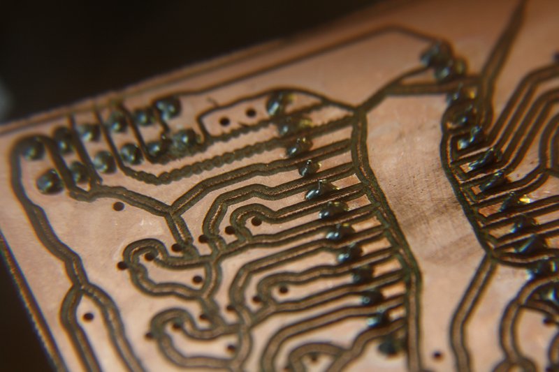
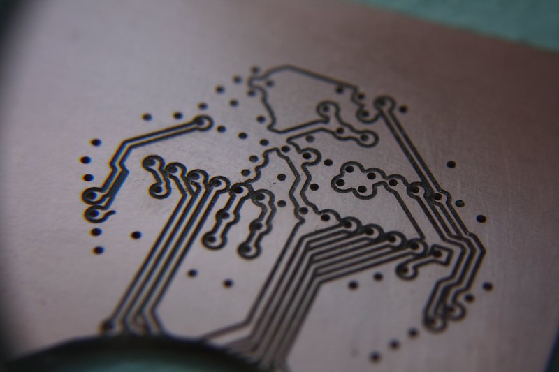
A mill with 0.5mm track width and clearance.
If you use an end mill that is the same diameter all the way up (not quite sure what the term is for these) then these tolerances are not going to cause problems - as long as you drill deep enough (I'm generally going down to -0.15mm or so), then you will get good traces. This is why we are restricted to a 0.5mm track clearance limit - thinner bits than this start to get too breakable to use. With proper auto-levelling you can use V shaped engraving bits instead, which get down to 0.1mm at the tip - but inconsistencies in Z will really mess this up as the cutting diameter will vary a lot as the height changes.
Don't mix your bits up
If you are clueless like me, it might be useful to point out that you use drills for making holes (going up and down only) and end mills (also sometimes known as burrs) to cut away material while moving across a surface. As mentioned above, the shape of an end mill is also critical - V shaped bits for example being specified by the angle in degrees.
This is what happens when you accidentally mill a board with a drill:
It's easy to mix up these tiny bits, but I won't do that again... I think the odd double tracks were caused by the drill bit bit being bent in the direction of its rotation! Most strangely of all - this board worked fine and is now in use, but it probably didn't do the drill bit much good.
Second attempt with the right tool for the job...
Once milled, the board can be soldered and needs to be protected from corrosion. If the copper is left unprotected, it gets tarnished quickly and starts to build up oxidisation within a few days. You can use fancy solder masks or "liquid tin" to coat the copper - but for the moment I'm just using clear nail varnish that seems to work for our purposes so far.
One thing that is missing that might be important for larger, more complex work is the screen printed layer on the top of the board that tells you where the components need to go. We've talked about CNC milling a lino or wood cut printing block with some form of registration that can be used to print on multiple boards.
Safety
While milling boards has advantages over etching (no need for acids or other dangerous chemicals that need disposing of) it's not a totally solved problem. The dust produced for example, is not the most healthy, so I've lately become something of a PCB material obsessive. A key factor here, is that things that affect our health are the same problems faced when these materials end up in landfill.
FR4 is the most common insulating material used as a substrate for copper clad boards. This is mainly a code name for its fire retardant properties (the most important aspect in terms of regulation for the finished product). These codes also seem to be used as a rough shorthand for the specific material used. Most of the time FR4 means fibreglass with an epoxy based resin, and this has two problems with regard to CNC milling. The first is that it's a very hard material so you get through your bits quickly, but the main problem is that fibreglass dust is damaging to your lungs, as the milling process chops the long, safe glass threads it contains into nasty microscopic fragments.
You can use a vacuum to control the dust, but this will need a high grade filter added to it - as otherwise it will make the problem worse as it just goes straight through and is sent back up into the air again.
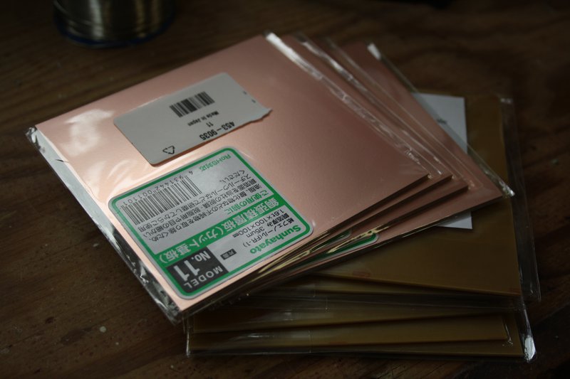
FR1 copper clad boards
Different materials are available for copper clad boards - older and cheaper (and less fire retardant) PCBs are called FR1 or FR2. These tend to be made from paper and phenolitic resin (also known as Bakelite). This is a softer material (so longer lasting CNC bits) and it removes the fibreglass problem entirely. However, there is now the phenolitic resin to worry about - this breaks down into phenol and formaldehyde, neither are particularly great for you, to say the least. These chemicals are detectable by smell well under their toxic concentrations, so this luckily means you are aware of them well before they are a problem. Interestingly these are the same "phenols" that are listed in the tasting notes in well peated whiskies, and a lot of people like the smell of old printed circuit boards! However - good ventilation is always important, whatever material you use.
I have managed to get hold of a couple of "FR2" copper clad boards that seem to be made from paper and epoxy, actually a cost saving measure which seems to be the safest combination - but these seem quite rare (and epoxy is probably not that safe itself).
A neat solution to all this which we're using is to drop a thin film of mineral oil on the copper surface first (it doesn't need much) This seems to capture most of the dust, and by nose - it seems to also stop most of the chemical elements escaping into the air, and is easy to clean up afterwards.
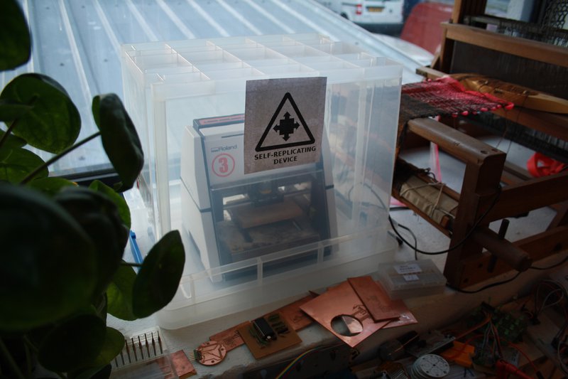
Another simple addition in the way of safety has been to put the whole thing in an upturned sealable box. This helps further reduce any dust and volatile compounds released, but also helps with noise. As complex boards can take over an hour to mill, the noise pollution involved, although not loud - is not inconsiderable in terms of irritation.
A failure (ran off the edge, and the laptop suspended halfway though) but good results for a more complex design.
At the moment we've been able to manufacture several working PCBs with this method, which saved us loads of time (mainly shipping) to increase turnaround for prototypes to well within a day. Also the minimum order size is usually 10-20 boards, so we save materials also. Designing and milling the board is considerably faster for anything non-trivial than using stripboard, and results in smaller boards too. For projects like the pattern matrix or woven swarm robots we need to produce many duplicates of the same PCB, which is where mass production has come in really useful - so the next test will be how many duplicates we can fit in a small printing footprint, and how consistent the results are.
Created: 15 Jul 2021 / Updated: 15 Jul 2021